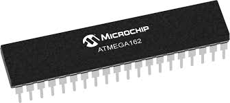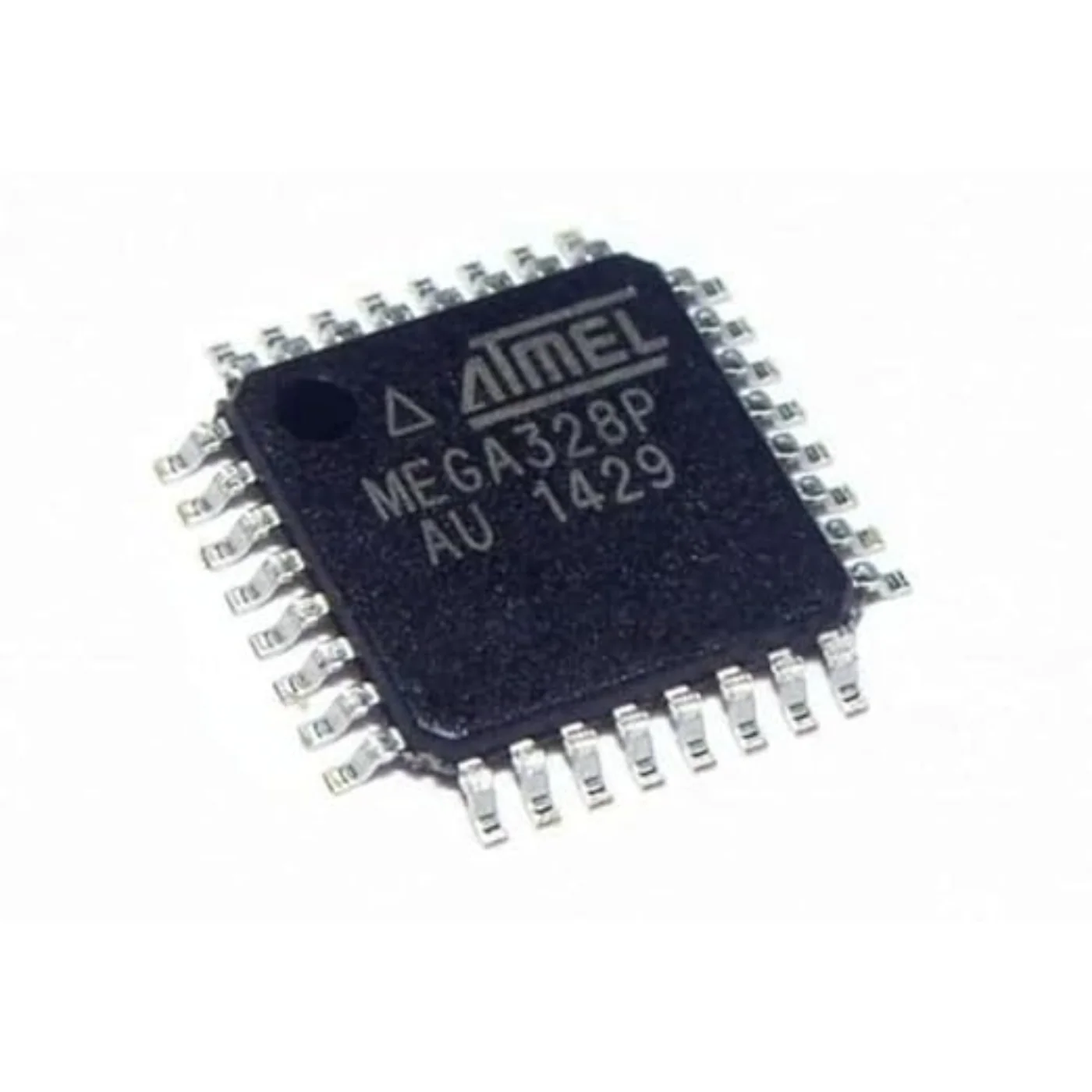
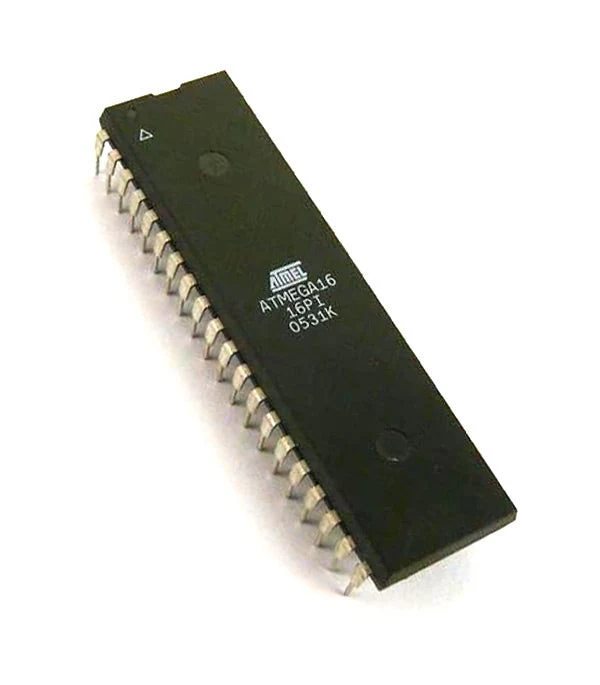
ATmega16
ATmega16
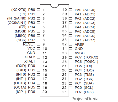
The ATmega ATmega16 is a low-power CMOS 8-bit microcontroller based on the AVR enhanced RISC architecture. By executing powerful instructions in a single clock cycle, the ATmega16 achieves throughputs approaching 1 MIPS per MHz allowing the system designer to optimize power consumption versus processing speed.
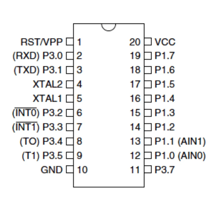
Pinout:

|
1 |
PB0(XCK/T0) |
Pin 0 of PORTB |
T0( Timer0 External Counter Input) XCK ( USART External Clock I/O) |
|
2 |
PB1(T1) |
Pin 1 of PORTB |
T1(Timer1 External Counter Input) |
|
3 |
PB2(INT2/AIN0) |
Pin 2 of PORTB |
AIN0(Internal Analog Comparator Positive Input) INT2( External Interrupt 2 Input) |
|
4 |
PB3(OC0/AIN1) |
Pin 3 of PORTB |
AIN1(Internal Analog Comparator Negative Input) OC0 (Timer0 Output Compare Match Output) or PWM output |
|
5 |
PB4(SS ) |
Pin 4 of PORTB |
SS (SPI Slave Select Input). This pin is low when controller acts as slave. [Serial Peripheral Interface (SPI) for programming] |
|
6 |
PB5(MOSI) |
Pin 5 of PORTB |
MOSI (Master Output Slave Input). When controller acts as slave, the data is received by this pin. [Serial Peripheral Interface (SPI) for programming] |
|
7 |
PB6(MISO) |
Pin 6 of PORTB |
MISO (Master Input Slave Output). When controller acts as slave, the data is sent to master through this pin. [Serial Peripheral Interface (SPI) for programming] |
|
8 |
PB7(SCK) |
Pin 7 of PORTB |
SCK (SPI Bus Serial Clock). This is the clock shared between this controller and other system for accurate data transfer. [Serial Peripheral Interface (SPI) for programming] |
|
9 |
RESET |
Reset Pin (Active Low Reset) |
|
|
10 |
VCC |
Connected to +5V |
|
|
11 |
GND |
Connected to GROUND |
|
|
12 |
XTAL2 |
Connected to Crystal Oscillator |
|
|
13 |
XTAL1 |
Connected to Crystal Oscillator |
|
|
14 |
PD0(RXD) |
Pin 0 of PORTD |
RXD (USART Input Pin) [USART Serial Communication Interface can be used for programming] |
|
15 |
PD1(TXD) |
Pin 1 of PORTD |
TXD (USART Output Pin) [USART Serial Communication Interface can be used for programming] |
|
16 |
PD2(INT0) |
Pin 2 of PORTD |
External Interrupt INT0 |
|
17 |
PD3(INT1) |
Pin 3 of PORTD |
External Interrupt INT1 |
|
18 |
PD4(OC1B) |
Pin 4 of PORTD |
OC1B (Timer Output Compare Match Output) or PWM output |
|
19 |
PD5(OC1A) |
Pin 5 of PORTD |
OC1A (Timer Output Compare Match Output) or PWM output |
|
20 |
PD6(ICP) |
Pin 6 of PORTD |
Timer/Counter1 Input Capture Pin |
|
21 |
PD7 (OC2) |
Pin 7 of PORTD |
Timer/Counter2 Output Compare Match Output |
|
22 |
PC0 (SCL) |
Pin 0 of PORTC |
TWI Interface |
|
23 |
PC1 (SDA) |
Pin 1 of PORTC |
TWI Interface |
|
24 |
PC2 (TCK) |
Pin 2 of PORTC |
JTAG Interface |
|
25 |
PC3 (TMS) |
Pin 3 of PORTC |
JTAG Interface |
|
26 |
PC4 (TDO) |
Pin 4 of PORTC |
JTAG Interface |
|
27 |
PC5 (TDI) |
Pin 5 of PORTC |
JTAG Interface |
|
28 |
PC6 (TOSC1) |
Pin 6 of PORTC |
Timer Oscillator Pin 1 |
|
29 |
PC7 (TOSC2) |
Pin 7 of PORTC |
Timer Oscillator Pin 2 |
|
30 |
AVcc |
Vcc for Internal ADC Converter |
|
|
31 |
GND |
GROUND |
|
|
32 |
AREF |
Analog Reference Pin for ADC |
|
|
33 |
PA7 (ADC7) |
Pin 7 of PORTA |
ADC (Analog to Digital Converter) Channel 7 |
|
34 |
PA6 (ADC6) |
Pin 6 of PORTA |
ADC (Analog to Digital Converter) Channel 6 |
|
35 |
PA5 (ADC5) |
Pin 5 of PORTA |
ADC (Analog to Digital Converter) Channel 5 |
|
36 |
PA4 (ADC4) |
Pin 4 of PORTA |
ADC (Analog to Digital Converter) Channel 4 |
|
37 |
PA3 (ADC3) |
Pin 3 of PORTA |
ADC (Analog to Digital Converter) Channel 3 |
|
38 |
PA2 (ADC2) |
Pin 2 of PORTA |
ADC (Analog to Digital Converter) Channel 2 |
|
39 |
PA1 (ADC1) |
Pin 1 of PORTA |
ADC (Analog to Digital Converter) Channel 1 |
|
40 |
PA0 (ADC0) |
Pin 0 of PORTA |
ADC (Analog to Digital Converter) Channel 0 |
Applications:
- Hobbyists applications
- Engineers design
- Temperature control systems
- Analog signal measuring and manipulations.
- Embedded systems like coffee machine, vending machine.
- Motor control systems.
- Digital signal processing.
- Peripheral Interface system.
Original: $2.25
-70%$2.25
$0.67More Images
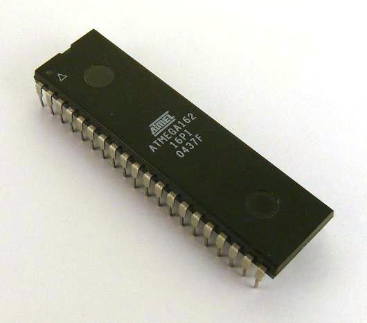
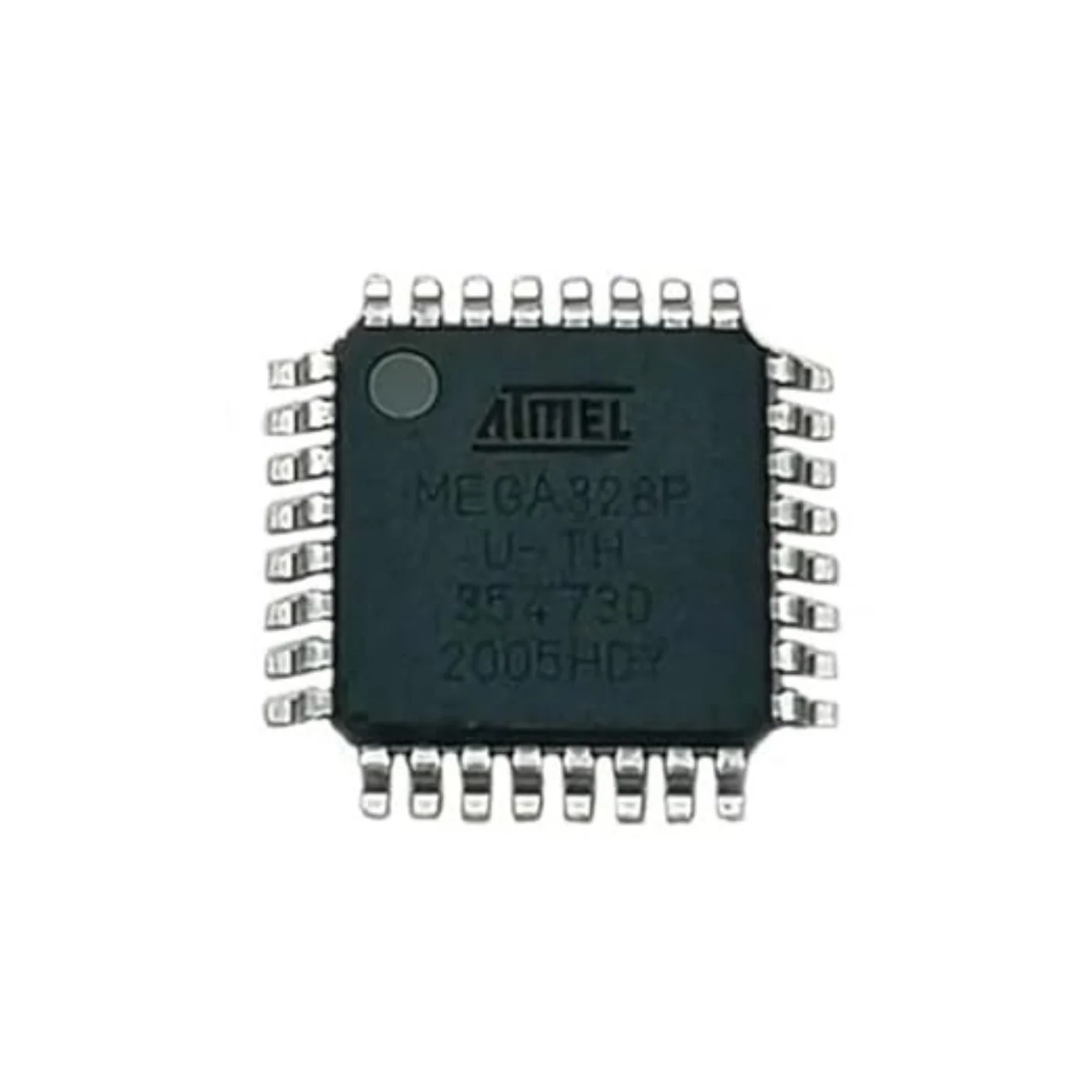
ATmega16
ATmega16
The ATmega ATmega16 is a low-power CMOS 8-bit microcontroller based on the AVR enhanced RISC architecture. By executing powerful instructions in a single clock cycle, the ATmega16 achieves throughputs approaching 1 MIPS per MHz allowing the system designer to optimize power consumption versus processing speed.
Pinout:
|
1 |
PB0(XCK/T0) |
Pin 0 of PORTB |
T0( Timer0 External Counter Input) XCK ( USART External Clock I/O) |
|
2 |
PB1(T1) |
Pin 1 of PORTB |
T1(Timer1 External Counter Input) |
|
3 |
PB2(INT2/AIN0) |
Pin 2 of PORTB |
AIN0(Internal Analog Comparator Positive Input) INT2( External Interrupt 2 Input) |
|
4 |
PB3(OC0/AIN1) |
Pin 3 of PORTB |
AIN1(Internal Analog Comparator Negative Input) OC0 (Timer0 Output Compare Match Output) or PWM output |
|
5 |
PB4(SS ) |
Pin 4 of PORTB |
SS (SPI Slave Select Input). This pin is low when controller acts as slave. [Serial Peripheral Interface (SPI) for programming] |
|
6 |
PB5(MOSI) |
Pin 5 of PORTB |
MOSI (Master Output Slave Input). When controller acts as slave, the data is received by this pin. [Serial Peripheral Interface (SPI) for programming] |
|
7 |
PB6(MISO) |
Pin 6 of PORTB |
MISO (Master Input Slave Output). When controller acts as slave, the data is sent to master through this pin. [Serial Peripheral Interface (SPI) for programming] |
|
8 |
PB7(SCK) |
Pin 7 of PORTB |
SCK (SPI Bus Serial Clock). This is the clock shared between this controller and other system for accurate data transfer. [Serial Peripheral Interface (SPI) for programming] |
|
9 |
RESET |
Reset Pin (Active Low Reset) |
|
|
10 |
VCC |
Connected to +5V |
|
|
11 |
GND |
Connected to GROUND |
|
|
12 |
XTAL2 |
Connected to Crystal Oscillator |
|
|
13 |
XTAL1 |
Connected to Crystal Oscillator |
|
|
14 |
PD0(RXD) |
Pin 0 of PORTD |
RXD (USART Input Pin) [USART Serial Communication Interface can be used for programming] |
|
15 |
PD1(TXD) |
Pin 1 of PORTD |
TXD (USART Output Pin) [USART Serial Communication Interface can be used for programming] |
|
16 |
PD2(INT0) |
Pin 2 of PORTD |
External Interrupt INT0 |
|
17 |
PD3(INT1) |
Pin 3 of PORTD |
External Interrupt INT1 |
|
18 |
PD4(OC1B) |
Pin 4 of PORTD |
OC1B (Timer Output Compare Match Output) or PWM output |
|
19 |
PD5(OC1A) |
Pin 5 of PORTD |
OC1A (Timer Output Compare Match Output) or PWM output |
|
20 |
PD6(ICP) |
Pin 6 of PORTD |
Timer/Counter1 Input Capture Pin |
|
21 |
PD7 (OC2) |
Pin 7 of PORTD |
Timer/Counter2 Output Compare Match Output |
|
22 |
PC0 (SCL) |
Pin 0 of PORTC |
TWI Interface |
|
23 |
PC1 (SDA) |
Pin 1 of PORTC |
TWI Interface |
|
24 |
PC2 (TCK) |
Pin 2 of PORTC |
JTAG Interface |
|
25 |
PC3 (TMS) |
Pin 3 of PORTC |
JTAG Interface |
|
26 |
PC4 (TDO) |
Pin 4 of PORTC |
JTAG Interface |
|
27 |
PC5 (TDI) |
Pin 5 of PORTC |
JTAG Interface |
|
28 |
PC6 (TOSC1) |
Pin 6 of PORTC |
Timer Oscillator Pin 1 |
|
29 |
PC7 (TOSC2) |
Pin 7 of PORTC |
Timer Oscillator Pin 2 |
|
30 |
AVcc |
Vcc for Internal ADC Converter |
|
|
31 |
GND |
GROUND |
|
|
32 |
AREF |
Analog Reference Pin for ADC |
|
|
33 |
PA7 (ADC7) |
Pin 7 of PORTA |
ADC (Analog to Digital Converter) Channel 7 |
|
34 |
PA6 (ADC6) |
Pin 6 of PORTA |
ADC (Analog to Digital Converter) Channel 6 |
|
35 |
PA5 (ADC5) |
Pin 5 of PORTA |
ADC (Analog to Digital Converter) Channel 5 |
|
36 |
PA4 (ADC4) |
Pin 4 of PORTA |
ADC (Analog to Digital Converter) Channel 4 |
|
37 |
PA3 (ADC3) |
Pin 3 of PORTA |
ADC (Analog to Digital Converter) Channel 3 |
|
38 |
PA2 (ADC2) |
Pin 2 of PORTA |
ADC (Analog to Digital Converter) Channel 2 |
|
39 |
PA1 (ADC1) |
Pin 1 of PORTA |
ADC (Analog to Digital Converter) Channel 1 |
|
40 |
PA0 (ADC0) |
Pin 0 of PORTA |
ADC (Analog to Digital Converter) Channel 0 |
Applications:
- Hobbyists applications
- Engineers design
- Temperature control systems
- Analog signal measuring and manipulations.
- Embedded systems like coffee machine, vending machine.
- Motor control systems.
- Digital signal processing.
- Peripheral Interface system.
Product Information
Product Information
Shipping & Returns
Shipping & Returns
Description
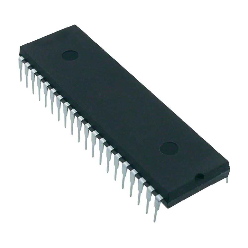
ATmega16
The ATmega ATmega16 is a low-power CMOS 8-bit microcontroller based on the AVR enhanced RISC architecture. By executing powerful instructions in a single clock cycle, the ATmega16 achieves throughputs approaching 1 MIPS per MHz allowing the system designer to optimize power consumption versus processing speed.
Pinout:
|
1 |
PB0(XCK/T0) |
Pin 0 of PORTB |
T0( Timer0 External Counter Input) XCK ( USART External Clock I/O) |
|
2 |
PB1(T1) |
Pin 1 of PORTB |
T1(Timer1 External Counter Input) |
|
3 |
PB2(INT2/AIN0) |
Pin 2 of PORTB |
AIN0(Internal Analog Comparator Positive Input) INT2( External Interrupt 2 Input) |
|
4 |
PB3(OC0/AIN1) |
Pin 3 of PORTB |
AIN1(Internal Analog Comparator Negative Input) OC0 (Timer0 Output Compare Match Output) or PWM output |
|
5 |
PB4(SS ) |
Pin 4 of PORTB |
SS (SPI Slave Select Input). This pin is low when controller acts as slave. [Serial Peripheral Interface (SPI) for programming] |
|
6 |
PB5(MOSI) |
Pin 5 of PORTB |
MOSI (Master Output Slave Input). When controller acts as slave, the data is received by this pin. [Serial Peripheral Interface (SPI) for programming] |
|
7 |
PB6(MISO) |
Pin 6 of PORTB |
MISO (Master Input Slave Output). When controller acts as slave, the data is sent to master through this pin. [Serial Peripheral Interface (SPI) for programming] |
|
8 |
PB7(SCK) |
Pin 7 of PORTB |
SCK (SPI Bus Serial Clock). This is the clock shared between this controller and other system for accurate data transfer. [Serial Peripheral Interface (SPI) for programming] |
|
9 |
RESET |
Reset Pin (Active Low Reset) |
|
|
10 |
VCC |
Connected to +5V |
|
|
11 |
GND |
Connected to GROUND |
|
|
12 |
XTAL2 |
Connected to Crystal Oscillator |
|
|
13 |
XTAL1 |
Connected to Crystal Oscillator |
|
|
14 |
PD0(RXD) |
Pin 0 of PORTD |
RXD (USART Input Pin) [USART Serial Communication Interface can be used for programming] |
|
15 |
PD1(TXD) |
Pin 1 of PORTD |
TXD (USART Output Pin) [USART Serial Communication Interface can be used for programming] |
|
16 |
PD2(INT0) |
Pin 2 of PORTD |
External Interrupt INT0 |
|
17 |
PD3(INT1) |
Pin 3 of PORTD |
External Interrupt INT1 |
|
18 |
PD4(OC1B) |
Pin 4 of PORTD |
OC1B (Timer Output Compare Match Output) or PWM output |
|
19 |
PD5(OC1A) |
Pin 5 of PORTD |
OC1A (Timer Output Compare Match Output) or PWM output |
|
20 |
PD6(ICP) |
Pin 6 of PORTD |
Timer/Counter1 Input Capture Pin |
|
21 |
PD7 (OC2) |
Pin 7 of PORTD |
Timer/Counter2 Output Compare Match Output |
|
22 |
PC0 (SCL) |
Pin 0 of PORTC |
TWI Interface |
|
23 |
PC1 (SDA) |
Pin 1 of PORTC |
TWI Interface |
|
24 |
PC2 (TCK) |
Pin 2 of PORTC |
JTAG Interface |
|
25 |
PC3 (TMS) |
Pin 3 of PORTC |
JTAG Interface |
|
26 |
PC4 (TDO) |
Pin 4 of PORTC |
JTAG Interface |
|
27 |
PC5 (TDI) |
Pin 5 of PORTC |
JTAG Interface |
|
28 |
PC6 (TOSC1) |
Pin 6 of PORTC |
Timer Oscillator Pin 1 |
|
29 |
PC7 (TOSC2) |
Pin 7 of PORTC |
Timer Oscillator Pin 2 |
|
30 |
AVcc |
Vcc for Internal ADC Converter |
|
|
31 |
GND |
GROUND |
|
|
32 |
AREF |
Analog Reference Pin for ADC |
|
|
33 |
PA7 (ADC7) |
Pin 7 of PORTA |
ADC (Analog to Digital Converter) Channel 7 |
|
34 |
PA6 (ADC6) |
Pin 6 of PORTA |
ADC (Analog to Digital Converter) Channel 6 |
|
35 |
PA5 (ADC5) |
Pin 5 of PORTA |
ADC (Analog to Digital Converter) Channel 5 |
|
36 |
PA4 (ADC4) |
Pin 4 of PORTA |
ADC (Analog to Digital Converter) Channel 4 |
|
37 |
PA3 (ADC3) |
Pin 3 of PORTA |
ADC (Analog to Digital Converter) Channel 3 |
|
38 |
PA2 (ADC2) |
Pin 2 of PORTA |
ADC (Analog to Digital Converter) Channel 2 |
|
39 |
PA1 (ADC1) |
Pin 1 of PORTA |
ADC (Analog to Digital Converter) Channel 1 |
|
40 |
PA0 (ADC0) |
Pin 0 of PORTA |
ADC (Analog to Digital Converter) Channel 0 |
Applications:
- Hobbyists applications
- Engineers design
- Temperature control systems
- Analog signal measuring and manipulations.
- Embedded systems like coffee machine, vending machine.
- Motor control systems.
- Digital signal processing.
- Peripheral Interface system.